Equipments
The University of Tokyo's Research Center for Advanced Science and Technology promotes
collaborative activities.
Tours for junior high school, high school, and undergraduate students are offered several times a year upon request and have been well received.
If you are interested in our experimental apparatus, please feel free to contact Assistant Professor (Sotome).
Equipments
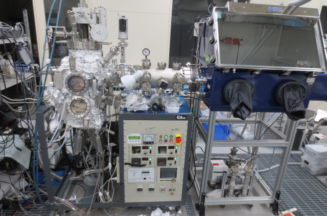
Vapor deposition equipment for perovskite type semiconductor 1
Equipped with four vapor deposition cells, it deposits perovskite-type semiconductors with gas and solid sources.
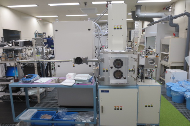
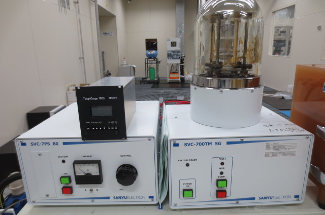
Vapor deposition equipment for perovskite type semiconductor 2
Equipped with 4 vapor deposition cells, it deposits perovskite type semiconductors.
Experimental results using this device have been used in the following papers and others:
H. Jung, Z. Liu, M. Sotome, and T. Kondo, "Vapor phase deposition of lead-free halide perovskite alloy CsSn1-xZnxBr3." Japanese Journal of Applied Physics, 63, 01SP24 (2024). DOI: 10.35848/1347-4065/acfdb3
Z. Liu, H. Jung, M. Sotome, and T. Kondo, "Substrate temperature dependence of vapor phase deposition of all-inorganic lead-free CsSnBr3 perovskite thin films." Japanese Journal of Applied Physics, 63, 01SP23 (2024). DOI: 10.35848/1347-4065/ad1196
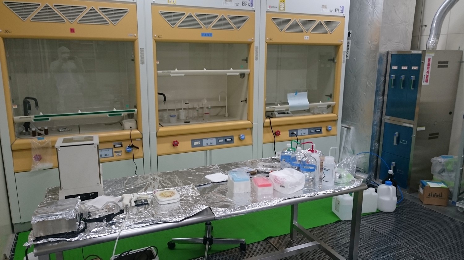
Air draft
Within it, we grows crystals from a solution.
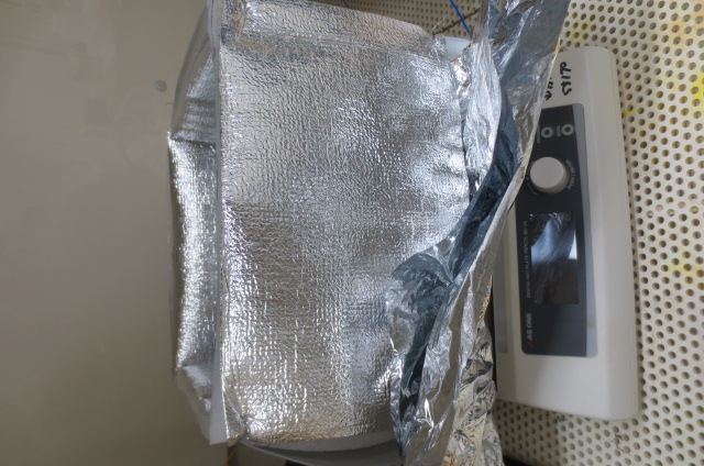
Hotplate 1
Temperature is controlled with an accuracy of 0.1 degree and crystals are grown slowly.
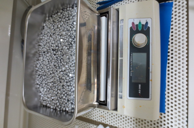
Hotplate 2
Crystals are grown by precisely controlling temperature in a bead bath.
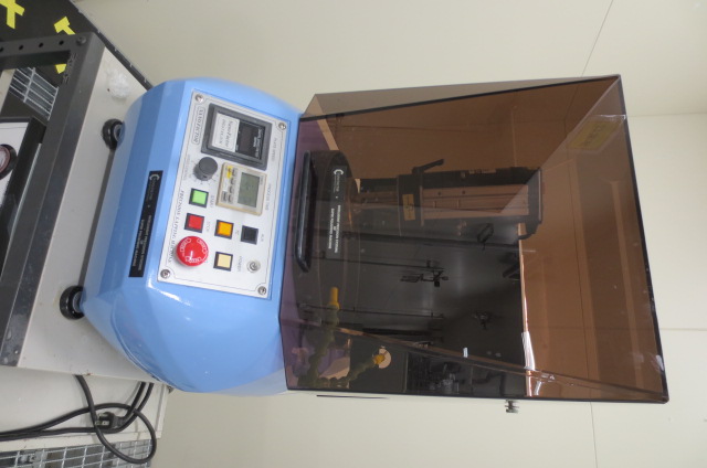
Crystal polisher
This device polishes crystals (CMP).
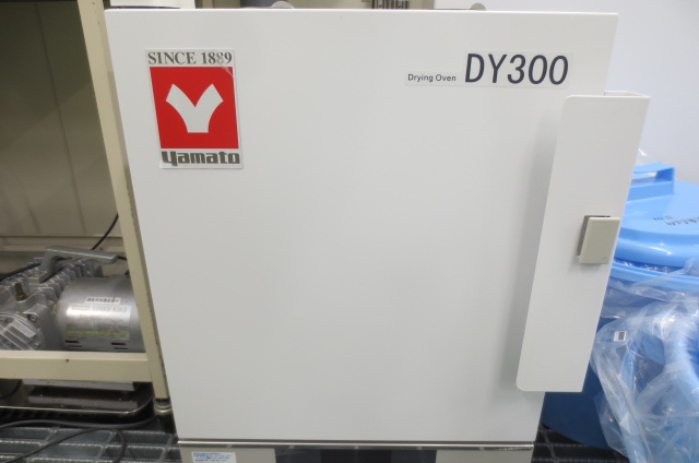
Dry Oven 1
This equipment is used for thermal annealing of samples.
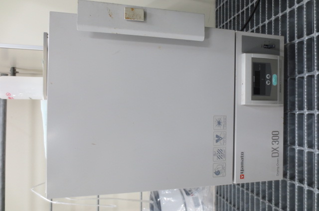
Dry Oven 2
This equipment is used for thermal annealing of samples.
spin coater
This equipment is used to spin-coat perovskite semiconductors and electrified transport layers.
With this equipment, the metal is heated and the metal layer for the electrode is vacuum deposited with an accuracy of 1Å.
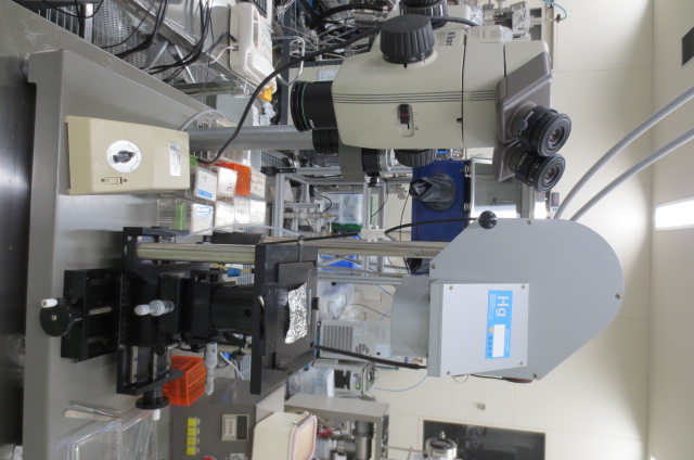
UV Exposure System
Expose the resist with a Hg light.
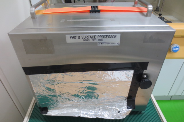
UV-Ozone equipments
This equipment cleans the substrate surface with UV light and UV-Ozone.
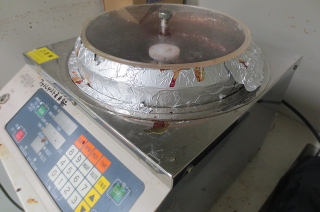
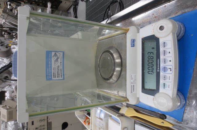
Electronic balance
This device precisely weighs raw materials and samples.
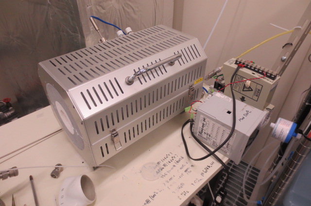
Heater furnace
This equipment is used to heat and sublimate the material to obtain a high purity raw material.
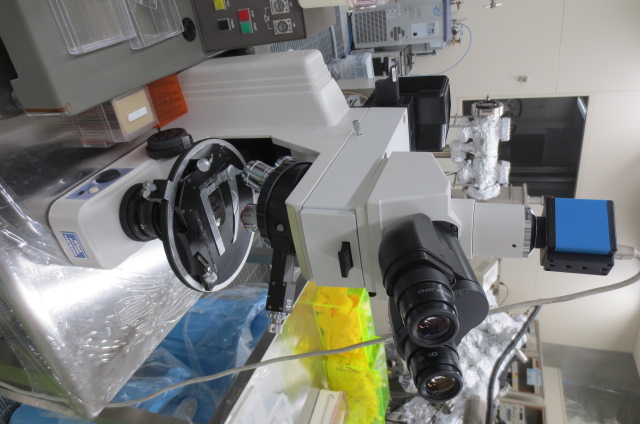
This device is used to magnify the image up to 100 times.
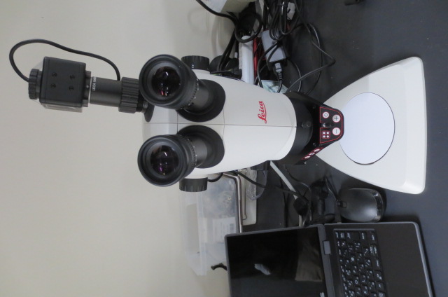
Stereomicroscope
This device facilitates electrode attachment and other operations.
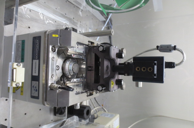
Atomic force microscope (AFM)
This device is used to observe the microscopic structure of thin films.
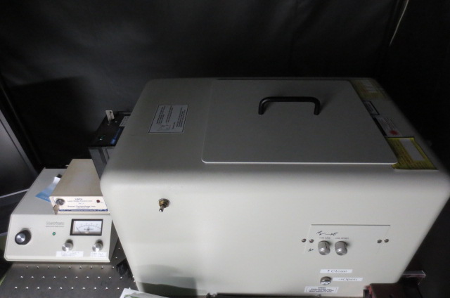
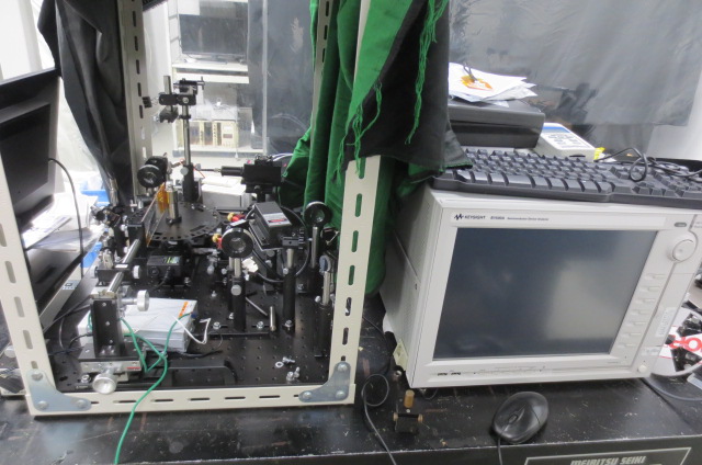
laser-excited photoluminescence spectroscopy
The sample is excited by lasers of various wavelengths and its emission is observed. The emission spectrum can be measured with a resolution of 0.1 nm while the sample is cooled down to a minimum temperature of 20 K. The results of experiments using this system have been used in the following papers::
Hui Chen, Yongsheng Ren, Masato Sotome, Takashi Kondo, and Kazuki Morita, "Solid solubility and site preference of Ti in 3C-and 6H-SiC". Materialia, 21, 101369 (2022). DOI: 10.1016/j.mtla.2022.101369.
Total Refractive Index Evaluation System
Evaluates refractive indices with high accuracy using total reflection.
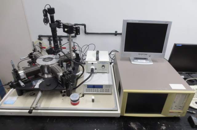
Low-temperature 4-terminal I-V measurement system
This device is used to perform 4-terminal measurements in a vacuum and at low temperatures.
AC Hall Measurement System
AC Hall measurement is performed to evaluate mobility with high accuracy even for high-resistance perovskite semiconductor samples. This is an advanced instrument with few commercially available products.
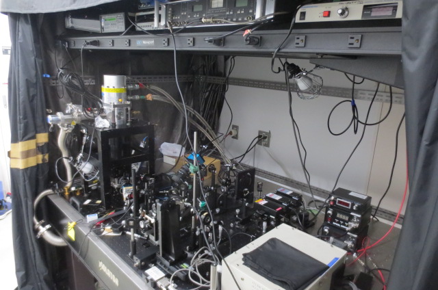
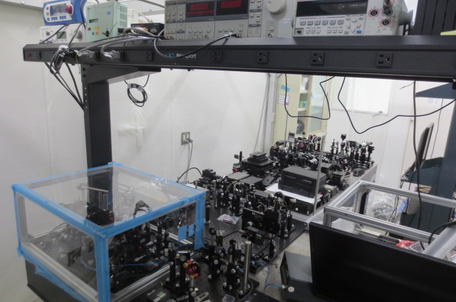
THz radiation experimental system
Experiments on terahertz wave generation and terahertz spectroscopy are performed using a 100fs fiber laser as a light source. 2 systems are available: a system using a 785nm fiber laser and a system using a 1560nm 100fs laser as a light source.
Experimental results using this system have been used in the following papers and others:
T. Noma, H. Y. Chen, B. Dhara, M. Sotome, T. Nomoto, R. Arita, M. Nakamura, D. Miyajima, "Bulk Photovoltaic Effect Along the Nonpolar Axis in Organic–Inorganic Hybrid Perovskites." Angewandte Chemie, e202309055 (2023). DOI: 10.1002/anie.202309055
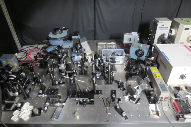
Microscopic transmission and reflection spectroscopy systems
Microscopically measure the transmittance and reflectance of a sample at 400-2000 nm.

