We are studying photonics materials and devices such as laser beam wavelength conversion devices using compound semiconductors GaAs and solar cells using perovskite type semiconductors.

We are growing compound semiconductors GaAs and perovskite-type semiconductor thin films by using molecular beam epitaxy (MBE), which is a thin film growth technology that can produce high-quality semiconductor crystals. It is possible to grow thin films with a composition and purity that are difficult to produce by other methods, such as a superlattice structure whose composition is controlled on a nanoscale.
Perovskite-type solar cell materials
Growth methods for halogenated perovskite single crystals and thin films
We are conducting research from the fabrication of halogenated perovskite single crystal thin films, which are expected to be used in light emitting / receiving devices.

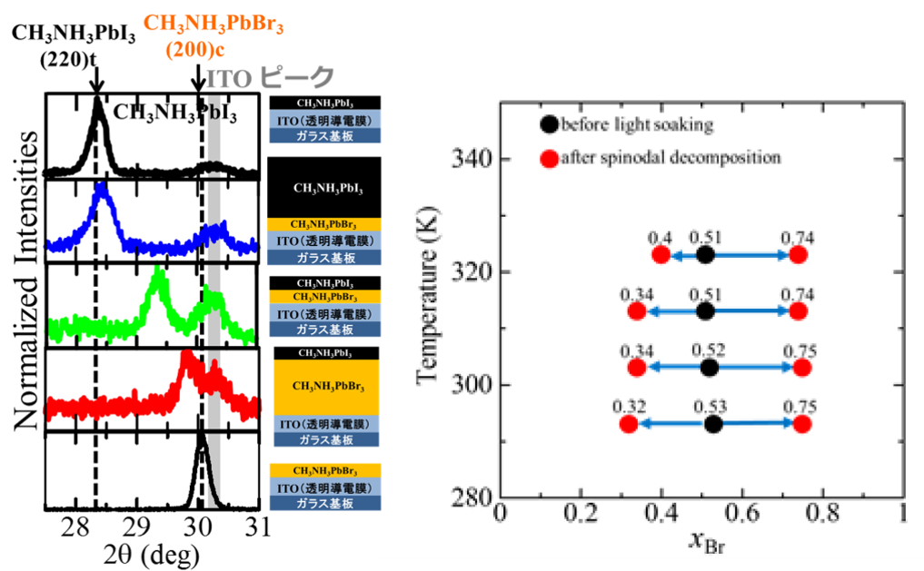
Spontaneous mixed crystallization and photoinduced spinodal decomposition
It was discovered that iodine-based CH3NH3PbI3 and bromine-based CH3NH3PbBr3 spontaneously co-crystallize when the halogenated lead perovskite polycrystalline thin film of iodine-based CH3NH3PbI3 and bromine-based CH3NH3PbBr3 is sequentially grown. We found that when the mixed crystal was irradiated with light, photo-induced spinodal decomposition occurred and separated into two types of compositions.
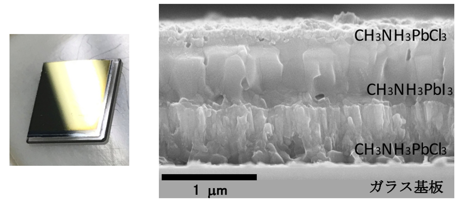
Double heterolayer film fabrication
We are conducting research to realize a tabular heteromembrane that is expected to be applied to light emitting devices by using polycrystalline thin films of iodine-based CH3NH3PbI3 and chlorine-based CH3NH3PbCl3, which are unlikely to be mixed with each other.
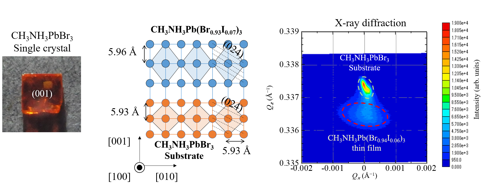
Fabrication of heteroepitaxial structure of perovskite semiconductors
We are conducting research to realize a halogenated perovskite single crystal thin film, which is expected to be used in light emitting / receiving devices.
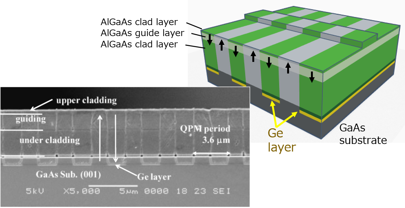
Sublattice-exchanged GaAs superlattice growth and wavelength conversion devices
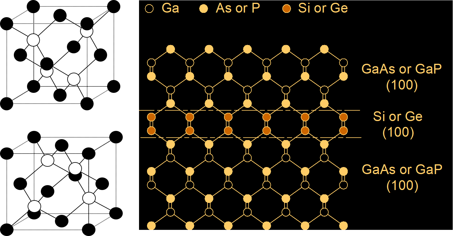
Researches of sublattice exchange epitaxy crystal growth
We are researching high-performance wavelength conversion devices that are expected to be applied to large-capacity optical communications and spectroscopy.
Waveguide type pseudo-phase matching wavelength conversion element
We are engaged in research on compound semiconductor crystal growth technology for wavelength conversion devices. Since compound semiconductors have extremely large nonlinear optical constants, they are excellent as wavelength conversion materials. We have independently developed and researched sub-lattice exchange epitaxy that controls the orientation of compound semiconductor crystals at the atomic level.
