HOME > Researches

We are researching semiconductor materials with potential applications in photonics by making full use of film formation methods that enable the fabrication of high-quality semiconductor crystals.

In particular, we are studying the physical properties of metal halide perovskite semiconductors, which are promising materials for high-efficiency, large-area thin-film solar cells, with the aim of understanding high-quality crystal growth and power generation mechanisms.

  • Preparation of Metal Halide Perovskite and Heterostructured Thin Films by Multi-source Co-Deposition
  • Study of photophysical properties of metal halide perovskite mixed crystals
  • Solar cells based on metal halide perovskite thin films
  • Nonlinear optical effects and quantum mechanical photocurrent in perovskite ferroelectric semiconductors
  • Terahertz wave generation from organic ferroelectrics and ferroelectric domain visualization
  • These are the main themes of our student-driven research.

    [Ongoing Research Topics...]

    Research on heteroepitaxial film fabrication

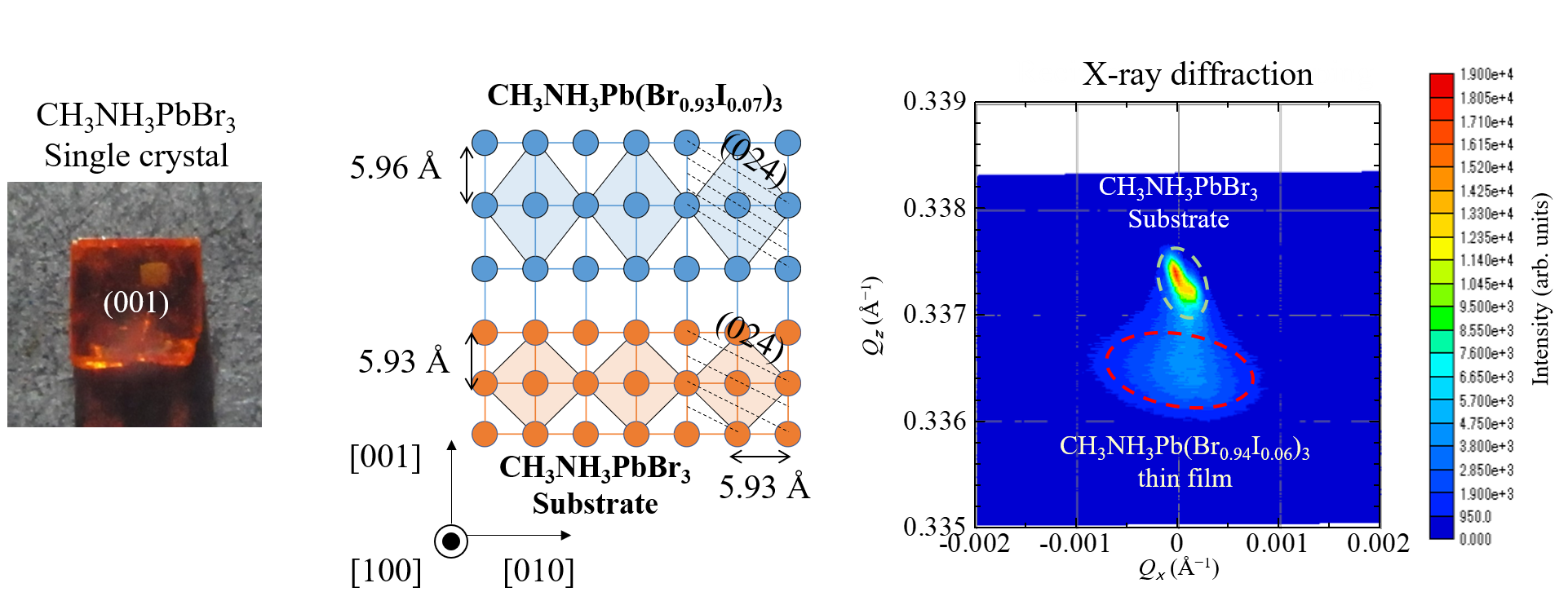
     We are studying heteroepitaxial thin films of halogenated perovskite thin films deposited on single crystals, which are expected to be used for light emitting and light receiving devices.
  • T. Matsushita, S. Takashima, Y. Nakamura, and T. Kondo, “Fabrication of CH3NH3PbI3/CH3NH3PbCl3 Heterostructure using Vacuum Evaporation,” 2018 International Conference on Solid State Devices and Materials (SSDM2018), September 9–13, 2018, The University of Tokyo, Tokyo,Japan (PS-6-11, Poster). etc.
  • Perovskite_heterostructure

    CH3NH3Pb(Br0.93I0.07)3Heteroepitaxial film growth of single crystal thin films

    Study of all-inorganic perovskite semiconductor thin film fabrication

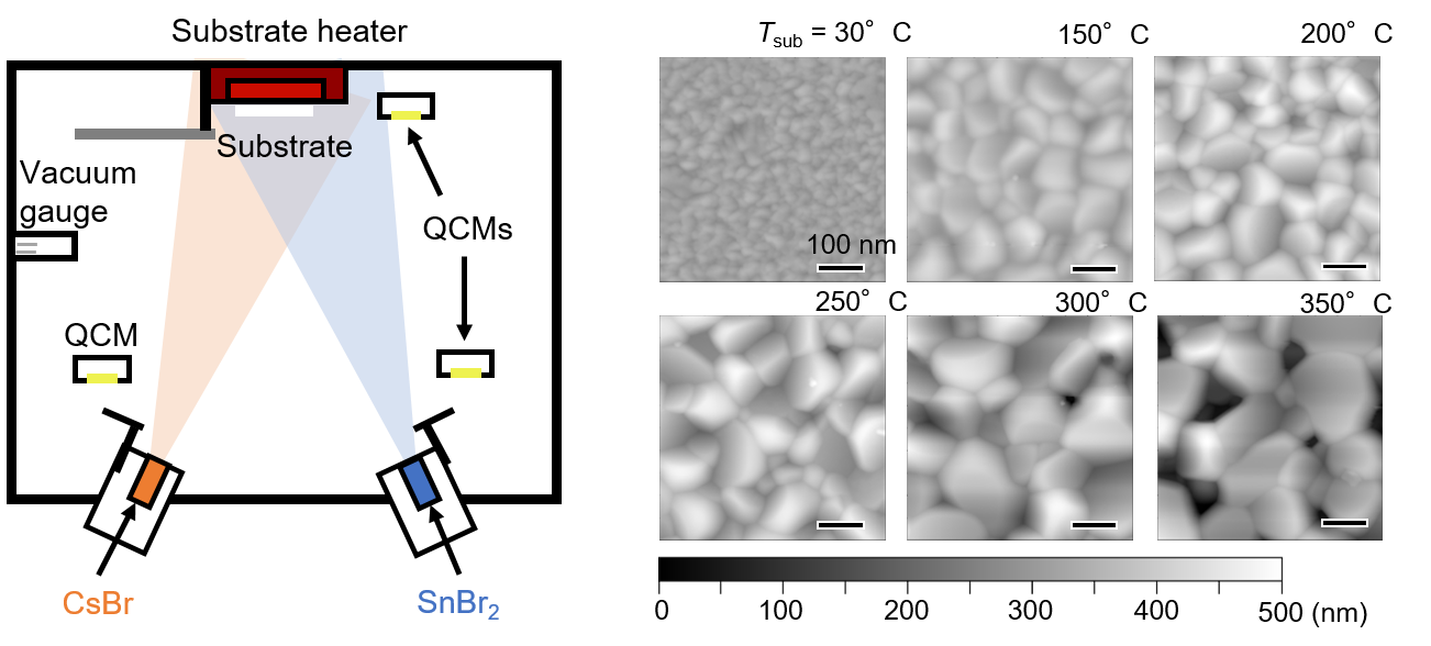
     We are conducting research on the fabrication of high-quality thin films of all-inorganic halogenated perovskite CsSnBr3 films, which are expected to have long-time stability and high environmental compatibility, by vacuum co-evaporation.
  • Z. Liu, H. Jung, M. Sotome, and T. Kondo, "Substrate temperature dependence of vapor phase deposition of all-inorganic lead-free CsSnBr3 perovskite thin films." Japanese Journal of Applied Physics, 63, 01SP23 (2024). DOI: 10.35848/1347-4065/ad1196
  • CsSnBr3 vapor deposition

    Study on the preparation of high-quality thin films of all-inorganic halide perovskite CsSnBr3 films by vacuum co-evaporation.

    Study of all-inorganic perovskite mixed crystal thin film fabrication

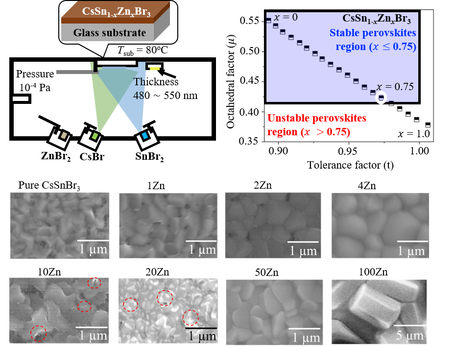
    We are studying the fabrication of high-quality thin films of Zn-doped all-inorganic halide perovskite CsSnBr3 films, which are expected to have long-time stability and high environmental compatibility, by vacuum co-evaporation and their application to solar cells.
  • H. Jung, Z. Liu, M. Sotome, and T. Kondo, "Vapor phase deposition of lead-free halide perovskite alloy CsSn1-xZnxBr3." Japanese Journal of Applied Physics, 63, 01SP24 (2024). DOI: 10.35848/1347-4065/acfdb3
  • CsSnZnBr3 vapor deposition

    Vacuum deposition study of all-inorganic halogenated perovskite CsSn1-xZnxBr3.

    Perovskite semiconductor double heterostructure thin film films

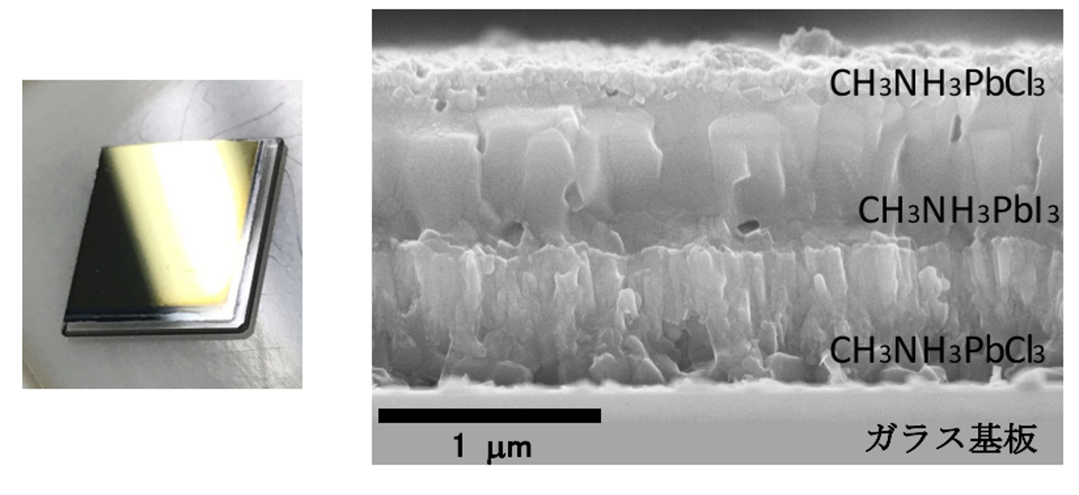
    We are conducting research to realize thin films with a tabular heterostructure, which is expected to be applied to light-emitting devices.
  • Shohei Toyota et al., "Fabrication of CsPbBr3/CsSnBr3/CsPbBr3 double heterostructure by vacuum co-deposition",. , The 83th JSAP Spring Meeting, 24p-22C-9 (2024).
  • T. Matsushita, S. Takashima, Y. Nakamura, and T. Kondo, “Fabrication of CH3NH3PbI3/CH3NH3PbCl3 Heterostructure using Vacuum Evaporation,” 2018 International Conference on Solid State Devices and Materials (SSDM2018), September 9–13, 2018, The University of Tokyo, Tokyo,Japan (PS-6-11, Poster). etc.
  • Fabrication_of_hetero-structure

    CH3NH3PbCl3/CH3NH3PbI3/CH3NH3PbCl3 double heterostructure thin film

    Terahertz wave generation from organic ferroelectrics and ferroelectric domain visualization

    We are studying terahertz wave generation by femtosecond laser irradiation and ferroelectric domain visualization using it in organic ferroelectrics, which are expected to be applied to next-generation electronics and photonics devices.
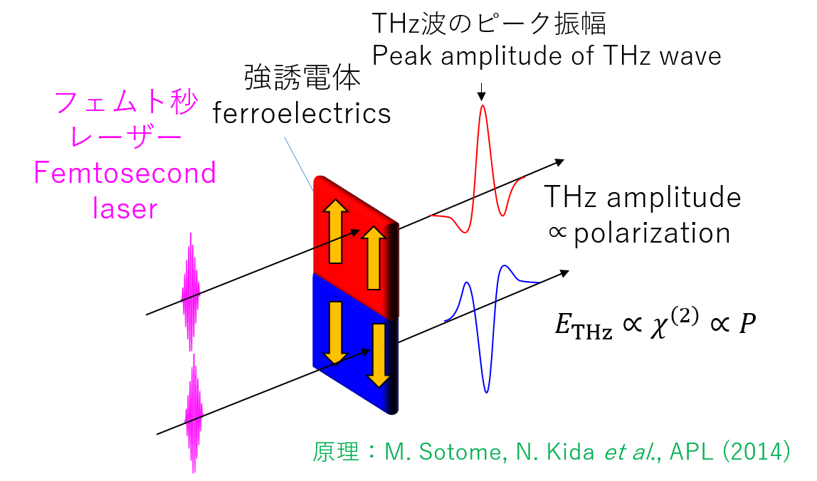
  • M. Sotome et al., "Three-dimensional visualization of the domain structure of molecular ferroelectrics [Hdabco][ReO4] by terahertz electromagnetic wave generation", The 84th JSAP Autumn Meeting, 20a-B203-6 (2023).
  • THz_img_schematics.png

    Principle diagram of ferroelectric domain visualization by THz wave generation.


    [History]


    Study of spoontaneous hybridization and photoinduced spinodal decomposition

    We found that sequential stacking of lead halide perovskite polycrystalline thin films of CH3NH3PbI3 (iodine-based) and CH3NH3PbBr3 (bromine-based) spontaneously hybridizes, while photo-induced spinodal decomposition occurs, separating the two compositions upon light absorption.
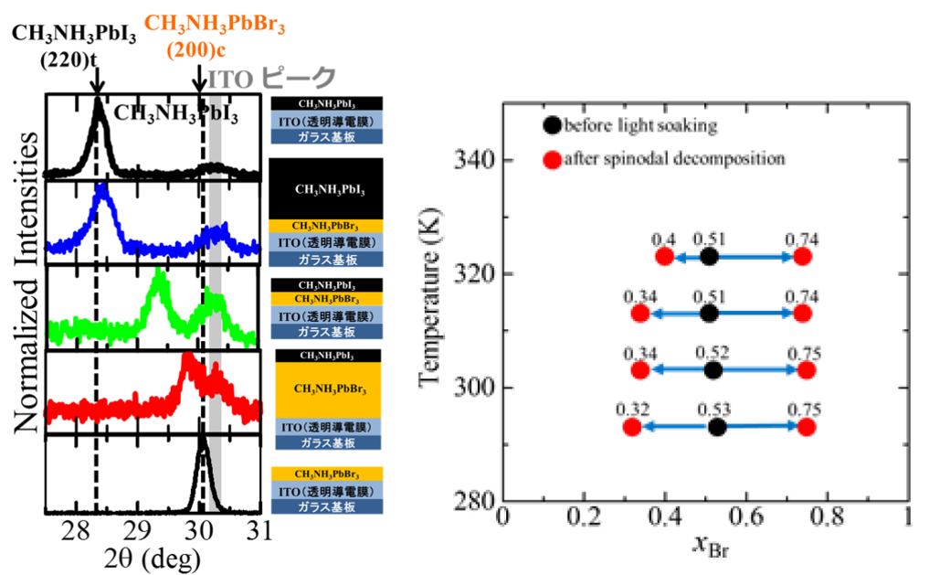
  • Y. Nakamura, N. Shibayama, A. Hori, T. Matsushita, H. Segawa, and T. Kondo, “Crystal systems and lattice parameters of CH3NH3Pb(I1-xBrx)3 determined using single crystals: Validity of Vegard’s law,” Inorg. Chem. 59, 6709–6716 (2020). DOI: 10.1021/acs.inorgchem.9b03421  etc..

  • Spinodal_phase_separation

    Spontaneous hybridization and photoinduced spinodal decomposition. (Left) X-ray diffraction patterns and respective thin film structures. (Right)Temperature dependence of photoinduced spinodal decomposition.

    Sublattice-exchanged GaAs superlattice growth and wavelength conversion devices

      We have researched the high-performance wavelength conversion devices that are expected to be applied to large-capacity optical communications and spectroscopy.
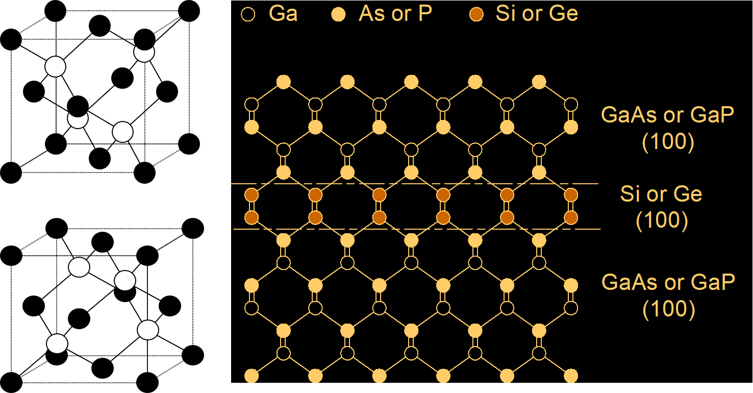
  • J. Ota, W. Narita, I. Ohta, T. Matsushita, and T. Kondo: “Fabrication of Periodically-Inverted AlGaAs Waveguides for Quasi-Phase-Matched Wavelength Conversion at 1.55 µm,” Jpn. J. Appl. Phys. 48, 04C110-1–4 (2009). DOI: 10.1143/JJAP.48.04C110. etc.
  • GaAs_sublattice_exchange_

      Crystal structure in a GaAs thin film grown by sublattice exchange epitaxy that controls the orientation of compound semiconductor crystals at the atomic level

    Waveguide type pseudo-phase matching wavelength conversion element

    We researched the compound semiconductor crystal growth technology for wavelength conversion devices. Since compound semiconductors have extremely large nonlinear optical constants, they are excellent as wavelength conversion materials. We have independently developed and researched sub-lattice exchange epitaxy that controls the orientation of compound semiconductor crystals at the atomic level.
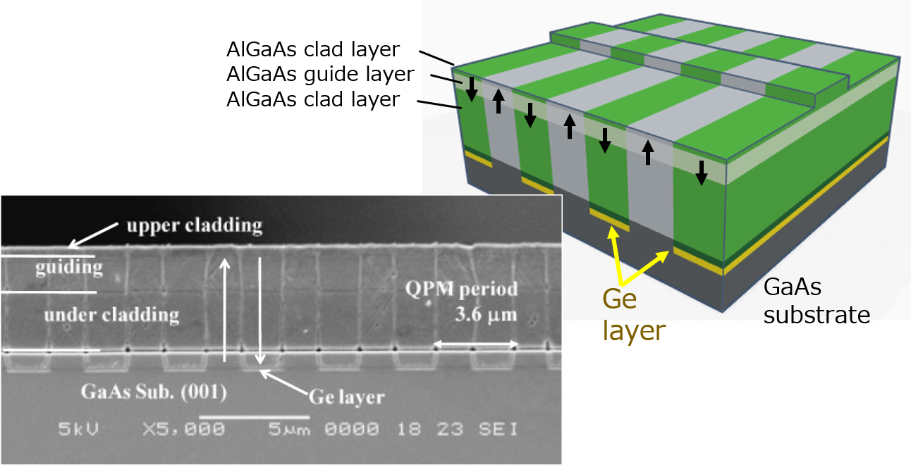
  • R. Narasaki, T. Matsushita, and T. Kondo, “Corrugation reduction in periodically inverted GaAs by molecular beam epitaxy growth using arsenic dimers,” Appl. Phys. Express 8, 025601-1–4 (2015). DOI: 10.7567/APEX.8.025601.  etc.

  • GaAs_wavelength_converter

    Structure of wavelength conversion device using periodic polarization inversion structure.


    Back to Page Top